
The Efficiency Revolution and Technology in Semiconductors
The Efficiency Revolution and Technology in Semiconductors
In the wave of semiconductor technology evolving towards high density and miniaturization, wafer-level packaging , with its innovative process logic, has become a core technology for breaking through the bottlenecks of traditional packaging. This technology, which emerged around 2000, overturned the traditional “dicing before packaging” model, injecting new vitality into the semiconductor industry through the reverse thinking of “packaging before dicing.”
The core logic of wafer-level packaging can be simply compared to this: traditional packaging is like cutting dough into small pieces and baking them separately, while wafer-level packaging is like baking a complete “big cake” first, and then dicing it into individual chips. This process revolution brings multiple advantages: the packaged chip size is almost 1:1 with the bare die, greatly increasing die density; the batch processing mode of whole wafers shortens the production cycle and significantly reduces average costs; more importantly, chip design and packaging design can be considered in an integrated manner, greatly improving development efficiency.
From a technical classification perspective, wafer-level packaging is mainly divided into two major directions: fan-in and fan-out. Fan-in packaging, as an early mainstream approach, has a package size identical to the chip, with wiring, insulating layers, and solder balls all concentrated on the top of the wafer, representing an important branch of chip-level packaging. Fan-out packaging, on the other hand, achieves size expansion by reconfiguring the wafer, supporting higher I/O density. Its post-chip processing improves yield to over 95%, making it the preferred choice for mid-to-high-end applications. Redistribution layers, as a core technology, act like “miniature circuit boards” within the package, allowing for flexible extension of electrical connections by rearranging I/O ports. Their linewidth has been reduced from the early 20μm to the 2μm level.
In terms of performance and application, wafer-level packaging demonstrates significant advantages. Electrically, shorter interconnect paths reduce signal delay and electromagnetic interference, resulting in 40% lower signal loss in the 28kHz band compared to traditional packaging, perfectly suited for 5G millimeter-wave applications. In terms of thermal management, material optimization and structural design effectively reduce chip operating temperature, improving reliability. Currently, this technology is widely used in smartphone processors, RF modules, automotive electronics, and is rapidly penetrating the Internet of Things and high-performance computing.
As the semiconductor industry enters the post-Moore’s Law era, wafer-level packaging is evolving towards higher integration and lower power consumption. The convergence of technologies such as heterogeneous integration and 3D stacking enables the integration of chips from different process nodes, achieving an optimal balance between functionality and cost. Industry forecasts predict that the global wafer-level packaging market will continue its rapid growth, becoming a key cornerstone supporting the development of emerging technologies and continuously driving electronic devices towards thinner, lighter, more efficient, and smarter designs.
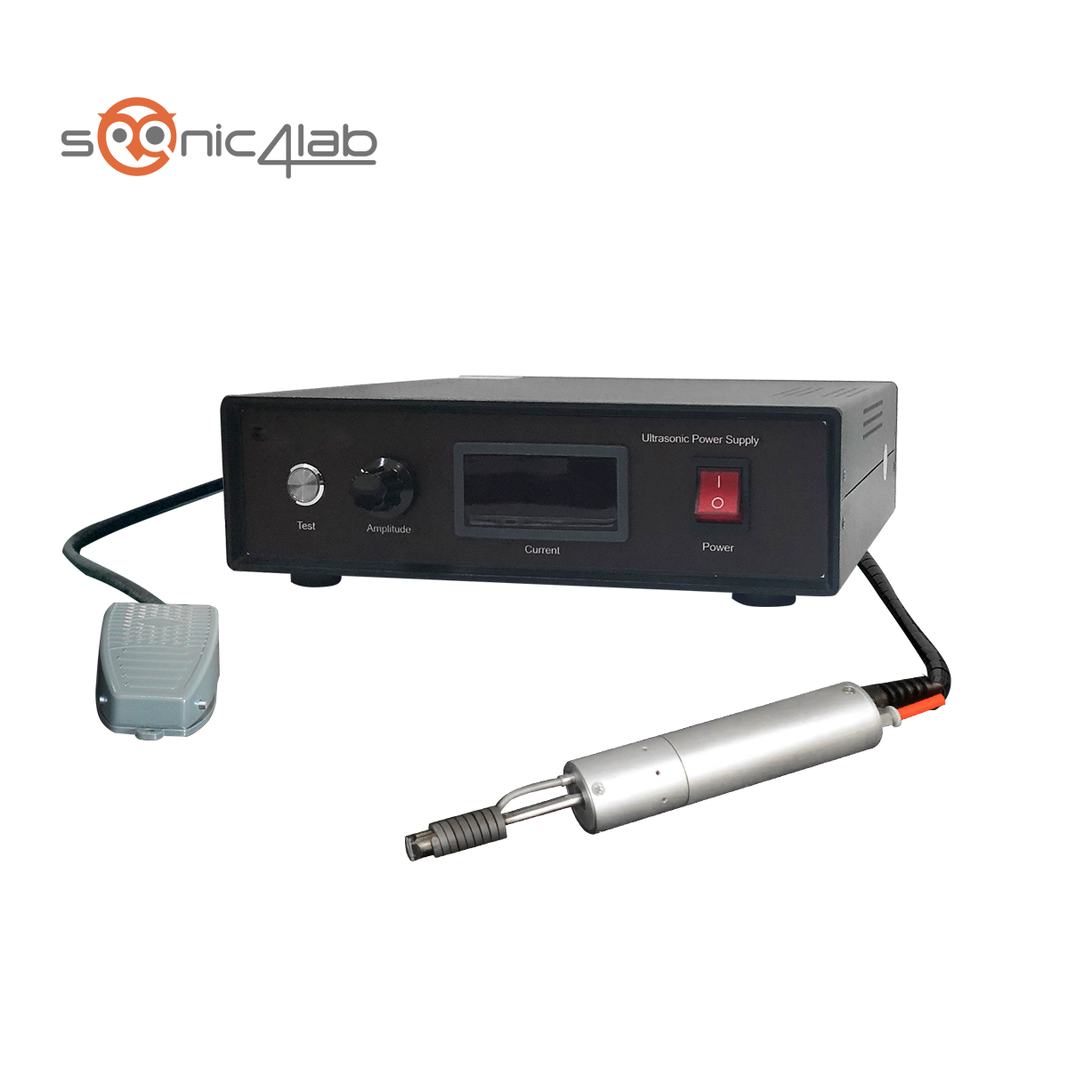
If you want to purchase equipment, please click here.
