
High Efficiency of Ultrasonic Wafer Copper Pillar Interconnects
High Efficiency of Ultrasonic Wafer Copper Pillar Interconnects
In the current era of rapid development in microelectronic packaging technology, the demand for precision and efficiency in wafer-level interconnect processes is increasingly prominent. Copper pillar bumps, with their excellent conductivity, thermal stability, and mechanical strength, have become a core choice for high-end chip interconnects. The emergence of ultrasonic soldering technology provides an innovative path for reliable connection of wafer copper pillar bumps, propelling the microelectronic packaging field towards a higher precision stage.
The core principle of ultrasonic soldering technology is to combine ultrasonic vibration energy with precise temperature-controlled heating to achieve a metallurgical bond between the copper pillar bumps and the substrate or chip pads. This technology transmits stable ultrasonic vibrations through the soldering iron tip, causing the oxide layer on the surface of the copper pillar bumps to break under mechanical vibration. Simultaneously, controlled temperature softens the metal interface, promoting atomic diffusion and lattice fusion, ultimately forming a dense, low-resistance interconnect. Compared to traditional thermoforming, ultrasonic soldering does not rely on a high-temperature environment and can complete the connection at a lower temperature, effectively avoiding thermal damage to the wafer chip caused by high temperatures. It is particularly suitable for high-end microelectronic devices with extremely high heat sensitivity requirements.
In wafer copper pillar interconnect scenarios, ultrasonic soldering bonding exhibits multiple core advantages. Firstly, it offers high connection precision, accurately matching the spacing requirements of micron-level copper pillar bumps. Positioning errors during bonding can be controlled at the micron level, meeting the process requirements of high-density packaging. Secondly, it provides strong interconnect reliability, resulting in a tight interface with low resistance and good stability, effectively reducing signal transmission loss and improving the electrical performance and long-term operational stability of devices. Thirdly, it offers broad process compatibility, applicable not only to pure copper pillar bumps but also to modified copper pillars such as tin-plated and gold-plated ones, and adaptable to substrates of different materials, supporting diverse packaging solutions. Fourthly, it boasts outstanding production efficiency, with short bonding cycles and simple equipment operation, facilitating automated mass production and meeting the cost control and efficiency requirements of large-scale microelectronics manufacturing.
Currently, this technology is widely used in the packaging processes of high-end microelectronic devices such as smartphone chips, automotive electronics, and industrial control chips. In 5G communication chip packaging, ultrasonic soldering bonding achieves high-density interconnection of copper pillar bumps, ensuring high-speed and stable signal transmission. In automotive power semiconductor packaging, its excellent mechanical strength and thermal stability meet the reliable operation requirements of automotive electronics under complex conditions.
As microelectronics technology continues to evolve towards miniaturization and high density, ultrasonic soldering bonding technology will also continue to upgrade. In the future, by optimizing ultrasonic vibration parameters, improving temperature control accuracy, and developing bonding tools adapted to smaller copper pillar bumps, this technology will further break through process limits, providing stronger support for the development of advanced packaging technologies and helping the microelectronics industry achieve higher-quality development.
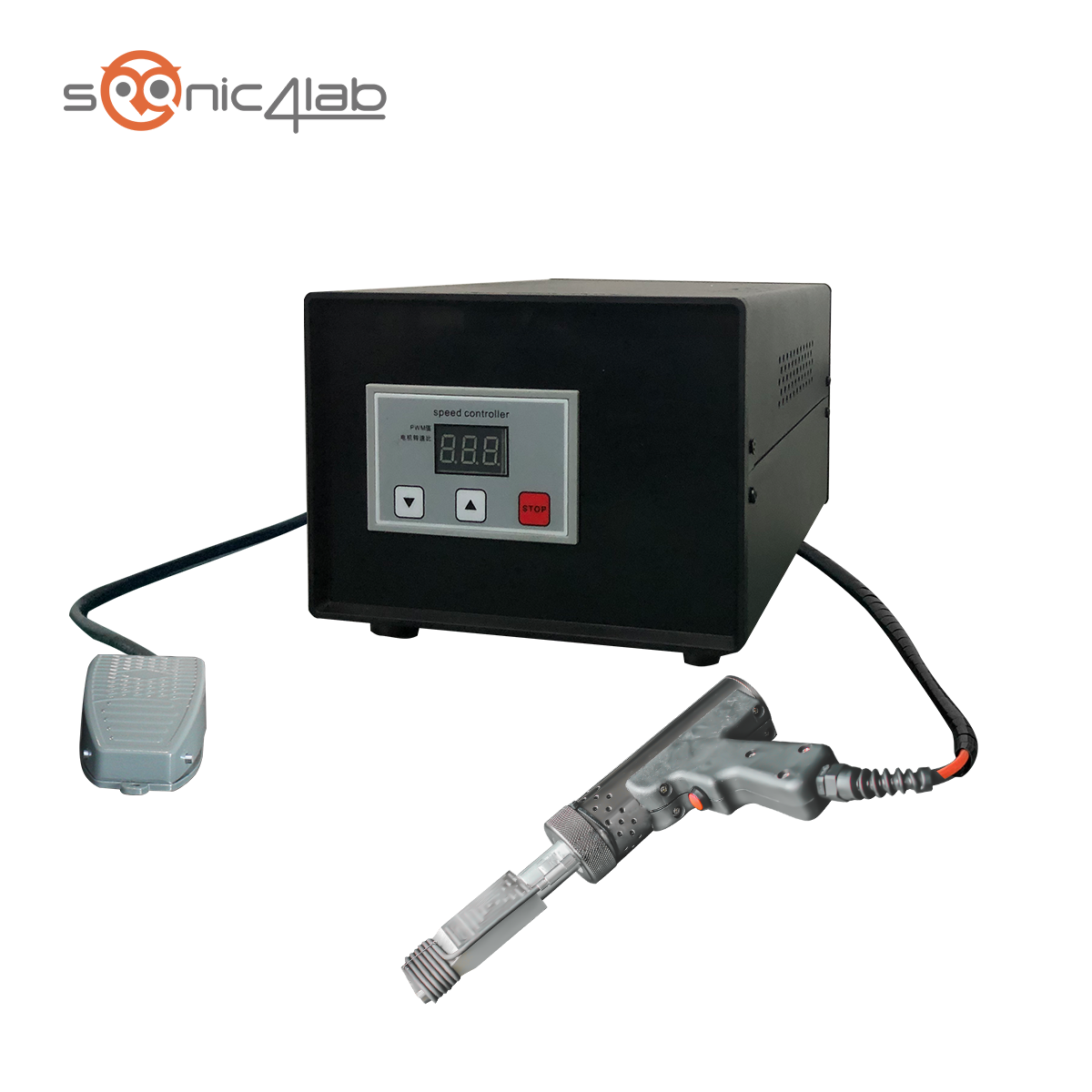
If you want to purchase equipment, please click here.
