
Ultrasonic Bonding of Sputtering Targets to Backing Plates Using Indium
Ultrasonic Bonding of Sputtering Targets to Backing Plates – Sonic4Lab
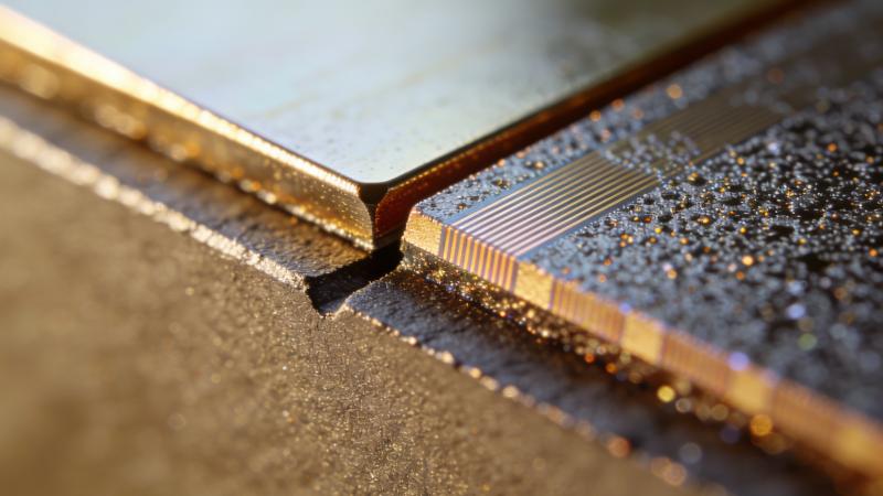
In the field of magnetron sputtering, the reliable bonding of sputtering targets to backing plates is a critical process that directly affects the performance and service life of sputtering equipment. Ultrasonic soldering bonding using indium as the solder has emerged as a preferred technology due to its unique advantages such as low-temperature operation, excellent bonding strength, and superior thermal conductivity. This article elaborates on the technical principles, process flow, key parameters, and performance advantages of this bonding method.
The core principle of ultrasonic soldering bonding lies in the synergistic effect of ultrasonic vibration and indium’s physical properties. Indium, with a low melting point of 156.6°C, exhibits excellent malleability and thermal conductivity, making it an ideal solder for bonding materials with different thermal expansion coefficients. During the bonding process, ultrasonic energy (typically in the frequency range of 15-35 kHz) is transmitted to the bonding interface through a sonotrode. This vibration generates two key effects: cavitation and mechanical scrubbing. Cavitation creates microbubbles in the molten indium, which collapse rapidly to produce localized high temperatures and pressure, promoting the wetting and spreading of indium on the surfaces of the target and backing plate. Mechanical scrubbing removes oxide films and contaminants from the bonding surfaces, ensuring direct contact between the indium and the base materials, thereby enhancing the bonding quality.
The ultrasonic soldering bonding process using indium involves several key steps, each requiring strict control to ensure bonding reliability. First, surface pretreatment of the sputtering target and backing plate is essential. The bonding surfaces need to be machined to a roughness of 3-5 μm, and then cleaned to remove oil, dust, and oxide layers. For some target materials such as graphite, a thin titanium film may be deposited on the bonding surface via vacuum magnetron sputtering to improve indium wettability. Subsequently, the backing plate is placed on a heating stage, and indium sheets (with a thickness of 0.6-3.0 mm) are evenly laid on the preprocessed bonding surface of the backing plate. The sputtering target is then accurately positioned on top of the indium sheets, and a moderate pressure is applied to ensure initial contact between the three layers.
The heating stage is then heated to 180-250°C to melt the indium sheets. Once the indium reaches a molten state, the ultrasonic transducer is activated, and the sonotrode is brought into contact with the target surface. The ultrasonic power is controlled within 300-500 W, and the vibration duration is set to 0.5-1.5 hours depending on the target size. During the ultrasonic vibration process, the molten indium is uniformly distributed over the entire bonding interface under the action of cavitation and mechanical scrubbing, filling microcracks and gaps. After the ultrasonic treatment is completed, the heating stage is gradually cooled to room temperature while maintaining the applied pressure. Finally, excess indium around the bonding interface is cleaned, and the bonding quality is inspected.
The control of key process parameters is crucial for achieving high-quality bonding. Ultrasonic power directly affects the intensity of cavitation and mechanical scrubbing: insufficient power may result in incomplete oxide film removal and poor indium wetting, while excessive power may cause damage to brittle target materials. The heating temperature must be strictly controlled above indium’s melting point but below the temperature that could degrade the target or backing plate materials; a temperature range of 180-250°C is generally optimal. The bonding pressure should be adjusted according to the target material’s hardness, typically in the range of 0.1-0.3 MPa, to ensure close contact without causing target deformation.

Compared with traditional bonding methods such as brazing and diffusion bonding, ultrasonic soldering bonding using indium offers significant advantages. Firstly, the low-temperature process minimizes thermal stress caused by differences in thermal expansion coefficients between the target and backing plate, reducing the risk of target cracking. Secondly, the ultrasonic vibration ensures a high bonding coverage rate (up to 98% or higher) and low void content (less than 2%), resulting in excellent thermal and electrical conductivity at the bonding interface. This efficient heat transfer is critical for dissipating the heat generated during sputtering, preventing solder leakage and target overheating. Additionally, the process is environmentally friendly as it avoids the use of flux, eliminating corrosion risks from residual flux. It also features simple operation, short processing time, and high adaptability to various target materials, including metal targets (such as WTi, NiV, Al) and ceramic targets.
Quality inspection after bonding is an indispensable step to ensure process reliability. Ultrasonic C-scan testing is commonly used to evaluate the bonding coverage rate and detect internal voids or unbonded areas. Shear strength testing is also performed to verify the bonding strength, with typical shear strengths exceeding 3300 psi. Cross-sectional microscopic analysis can further observe the indium distribution and interface bonding status, ensuring that the bonding meets the application requirements.
In conclusion, ultrasonic soldering bonding using indium provides a reliable, efficient, and low-damage solution for joining sputtering targets to backing plates. By strictly controlling the surface pretreatment, ultrasonic parameters, temperature, and pressure, high-quality bonding with excellent thermal conductivity and mechanical strength can be achieved. This technology not only improves the performance and service life of sputtering target assemblies but also supports the development of large-size and high-purity sputtering targets, playing a vital role in advancing the magnetron sputtering technology in fields such as semiconductor manufacturing and thin-film coating.
If you want to purchase equipment, please click here.

