
Applications of Ultrasonic Brazing System in Electronic Packaging
Applications of Ultrasonic Brazing System in Electronic Packaging – Sonic4Lab
Electronic packaging, as a core component for the functional realization and reliability assurance of electronic devices, places stringent requirements on the precision, low thermal damage, and high stability of the connection process. Ultrasonic brazing equipment, with its unique working mode of “ultrasonic vibration + thermo-pressure synergy,” effectively solves the pain points of traditional brazing processes in precision electronic packaging, such as thermal deformation and oxidation residue, becoming key equipment in fields such as semiconductors, automotive electronics, and 5G communications. Its core value lies in achieving reliable metallurgical connections between dissimilar materials through low-frequency high thermal efficiency or high-frequency high-precision energy control, adapting to diverse packaging needs from microchips to power modules.
The core components of ultrasonic brazing equipment revolve around energy conversion and precise control, mainly including four functional modules. The ultrasonic generation system is the energy core, converting power frequency electrical energy into high-frequency mechanical vibrations of 20-120kHz through a piezoelectric transducer. After amplification by an amplitude modulator, the vibration is transmitted to the welding head, and the vibration amplitude can be precisely controlled to 0.1-10μm to meet the energy requirements of different packaging scenarios. The precision motion control system employs linear motors and air bearings, achieving X/Y axis positioning accuracy of ±0.5-2μm and Z-axis pressure control accuracy of ±0.1N via a voice coil motor. Combined with a 4K vision alignment system, it can achieve sub-micron level solder joint positioning, suitable for fine-pitch lead (<20μm) packages. The thermo-pressing collaborative system uses infrared temperature measurement and PID algorithms to stably control the bonding temperature between 150-300℃, achieving low-temperature interconnection and avoiding high-temperature damage to chip performance. The real-time monitoring system provides closed-loop feedback on parameters such as ultrasonic power, pressure, and deformation, keeping the welding defect rate below 0.01%.
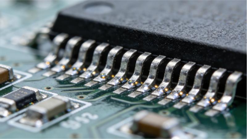
In the field of electronic packaging, ultrasonic brazing equipment offers significant technological advantages. Firstly, its low-temperature interconnection characteristics significantly reduce thermal damage. Compared to the high temperatures of traditional fusion soldering (above 300℃), its operating temperature of 150-250℃ is suitable for temperature-sensitive chips such as CMOS and optoelectronic devices, avoiding stress residue caused by mismatched thermal expansion coefficients of packaging materials. Secondly, the absence of oxide residue ensures reliable connections. The high-frequency friction of ultrasound can break down the oxide film on the solder pad surface, achieving a clean interface connection without flux. This reduces interference from residual impurities in signal transmission, making it particularly suitable for high-frequency communication device packaging. Thirdly, high precision adapts to the trend of high-density packaging. It can handle various bonding wires such as gold, silver, and copper with diameters of 10-75μm, with a wire arc control accuracy of ±1μm, meeting the fine-pitch connection requirements of advanced processes such as multi-chip stacking and 3D packaging.

Based on these advantages, ultrasonic brazing equipment has formed diversified application scenarios in electronic packaging. In the field of semiconductor packaging, high-frequency ultrasonic brazing equipment undertakes the task of wire bonding between chips and substrates. It achieves submicron-level interconnection through 120kHz high-frequency vibration, and the signal transmission loss can be controlled below 0.5dB/cm, making it suitable for high-end device packaging such as 5G base station optical modules and quantum chips. In the automotive electronics field, for the packaging requirements of IGBT and SiC power modules, the equipment achieves reliable connections between copper wires and metal substrates through a wide-range pressure control system of 10-30N and a nitrogen protection system, reducing module thermal resistance by 20% and extending service life to 150,000 hours. In power semiconductor packaging, pin ultrasonic soldering equipment replaces traditional solder paste soldering, improving connection stability through metal covalent bonding. It maintains stable thrust even after 15G acceleration vibration testing, meeting automotive-grade reliability standards.
Currently, ultrasonic soldering equipment is upgrading towards intelligence and high integration. By integrating AI visual positioning and path planning algorithms, the equipment can achieve automatic solder joint calibration and defect identification, increasing yield to over 99.99%. The application of a distributed motion control architecture shortens the data refresh cycle of the soldering, conveying, and inspection modules to 250μs, significantly improving mass production efficiency. Simultaneously, for the packaging requirements of third-generation semiconductor materials, the equipment uses a three-stage energy progressive loading technology to reduce soldering pressure by 40% while ensuring connection strength, further expanding application boundaries. In the future, as electronic packaging develops towards miniaturization and high density, ultrasonic brazing equipment will continue to make breakthroughs in areas such as adaptive parameter control and multi-material compatibility, providing core equipment support for the technological upgrading of the electronic information industry.
If you want to purchase equipment, please click here.

