
Defect-Free Joining of Sputtering Targets and Backplanes
Application of Ultrasonic Welding Systems in Defect-Free Joining of Sputtering Targets and Backplanes
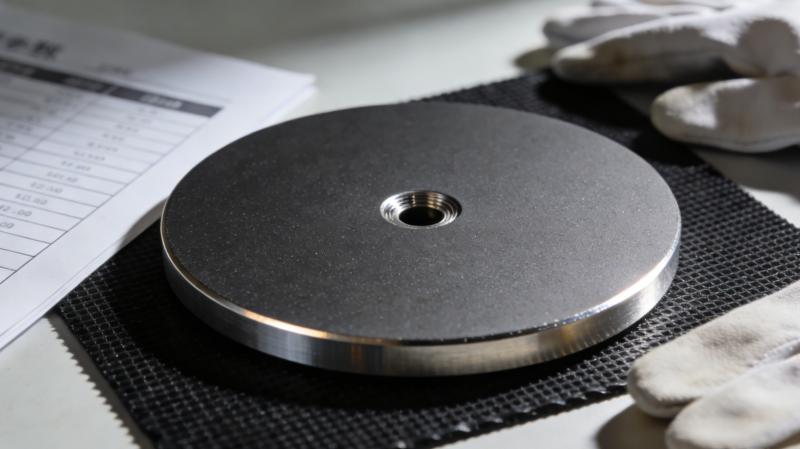
In high-tech fields such as semiconductors, photovoltaics, and display panels, the quality of the join between sputtering targets and backplanes directly determines device performance and lifespan. During sputtering, the backplane plays a crucial role in supporting the target and efficiently conducting heat. Pores or cracks in the joint can lead to serious problems such as excessively high local temperatures, target detachment, and even uneven film deposition. Ultrasonic welding systems, with their unique flux-free and low-damage welding characteristics, have become a core technology for achieving defect-free joining between sputtering targets and backplanes, providing reliable assurance for precision machining in high-end manufacturing.
The core principle of ultrasonic welding systems in achieving pore-free and crack-free joints lies in the synergistic effect of ultrasonic cavitation and mechanical vibration. Unlike traditional welding processes that rely on high-temperature melting of the solder, this system uses high-frequency ultrasonic vibration (typically 20-60kHz) to act on the molten solder layer, inducing intense cavitation. During the formation and instantaneous collapse of cavitation bubbles, localized high pressure and microjets are generated, acting like a “microscopic brush” to efficiently remove oxide layers and contaminants from the target and backing surfaces, achieving direct wetting of the solder and substrate without the need for corrosive flux. This physical cleaning mechanism not only avoids joint corrosion and porosity defects caused by flux residue but also significantly enhances the solder’s wetting ability, laying the foundation for dense joint formation.
During the welding process, ultrasonic vibration further promotes uniform solder spread and gap filling. Under high-frequency vibration, the fluidity of the molten solder is significantly enhanced, allowing it to be efficiently pressed into the tiny gaps and micropores on the substrate surface, achieving complete interface adhesion and sealing. Simultaneously, the vibration energy effectively expels gas bubbles from the solder layer, suppressing porosity defects at their source. Compared to traditional brazing processes, which are prone to thermal stress cracking due to differences in thermal expansion coefficients, the localized heating characteristics of ultrasonic welding can significantly reduce the temperature gradient between the target and backing. Especially for joining dissimilar materials such as copper, aluminum, and titanium, its low heat input advantage reduces thermal deformation, avoids crack initiation and propagation caused by stress concentration, and ensures the integrity of the joint structure.
Achieving defect-free bonding between sputtering targets and backing plates requires precise control of key process parameters of the ultrasonic welding system. Parameters such as ultrasonic power, vibration frequency, welding time, solder extrusion rate, and the height of the welding head from the substrate work synergistically and directly affect joint quality. For example, for bonding ITO targets to copper backing plates, using ultrasonic energy at a frequency of 35kHz and a power of 1000-1400W, combined with a 20-40 minute immersion treatment, allows the indium solder to penetrate uniformly into the interface layer, increasing the bonding rate to over 97%. Solder selection is equally crucial. Indium-based solders, due to their good ductility and thermal conductivity, are often used for target bonding. By controlling the solder layer thickness to 2-5mm and using copper wire with a diameter of 0.5-0.6mm as a support structure, the uniformity of solder distribution can be further optimized, reducing the defect rate. Furthermore, masking the non-welding surfaces of the target and backplate before welding, followed by air cooling to room temperature after welding, effectively avoids secondary contamination and residual thermal stress.

The application of ultrasonic welding systems in sputtering target bonding has significantly promoted process upgrades in high-end manufacturing. In semiconductor chip manufacturing, the defect-free bonding of high-purity metal targets to copper alloy backplates ensures the uniformity and stability of sputtered thin films, facilitating the evolution of chip manufacturing processes towards the nanometer scale. In the photovoltaic field, this technology enables reliable encapsulation of transparent conductive film targets, improving the photoelectric conversion efficiency and lifespan of solar cells. Its flux-free, low-damage, and high-consistency characteristics not only reduce the cost of subsequent cleaning processes but also reduce environmental pollutant emissions, aligning with the trend of green manufacturing. With the integration of automation technology, modular ultrasonic welding systems can achieve precise replication of process parameters and large-scale production, providing customized solutions for bonding targets and backplates of different materials and shapes, further expanding its application scenarios.
In summary, ultrasonic welding systems, through their unique cavitation effect and precise process control, effectively solve core defect problems such as porosity and cracks in the connection between sputtering targets and backplanes. Their significant advantages in joining dissimilar materials, low thermal stress, environmental friendliness, and high efficiency make them a key technology for manufacturing high-end sputtering targets and components. With technological advancements, this system will continue to be upgraded in areas such as process parameter optimization and intelligent control, providing stronger technical support for the high-quality development of high-tech industries.
If you want to purchase equipment, please click here.

