
The Core of Substrate Interconnect Electronic Devices
The Core of Substrate Interconnect Electronic Devices – Sonic4lab
In the wave of miniaturization, high frequency, and high reliability upgrades in electronic devices, substrate interconnect, as the “neural network” hidden within the device, undertakes the critical missions of signal transmission, power supply, and structural support. Its technological level directly determines the performance ceiling and development space of electronic products, becoming the core hub connecting core chips and terminal devices.
The core value of substrate interconnect lies in achieving stable connections between different circuit layers through precise interlayer alignment and efficient conductivity design, breaking the limitations of traditional interconnect modes. Compared with ordinary interconnect technologies, advanced substrate interconnect solves the signal transmission challenges of high-density, multi-layer substrates with micron-level precision control. Its interlayer alignment error can be controlled within tens of micrometers, finer than a human hair, ensuring the stable operation of complex circuits and avoiding problems such as signal interruption and short circuits.
Diverse interconnect processes provide flexible solutions for applications in different scenarios. Through-hole vias, as the most basic interconnect method, are widely used in low- to mid-range multilayer substrates due to their cost-effectiveness, achieving full-layer connectivity much like a straight staircase in architecture. Blind vias and buried vias focus on efficient interconnection of high-layer substrates, saving significant space by not penetrating the entire substrate and meeting the needs of miniaturized devices. Laser-guided micro-blind vias further elevate precision to new heights, with tiny apertures enabling hundreds of interconnect points per square centimeter, significantly improving signal transmission speed and reducing losses.
The iteration of substrate interconnect technology is driving industrial upgrades in multiple fields. In the communications field, high-layer substrates in 5G base stations achieve high-speed, lossless signal transmission through precise inter-layer interconnect design, supporting increased base station data processing capacity. In automotive electronics, automotive substrate interconnect technology can withstand harsh environments such as high temperatures and vibrations, enabling real-time interconnection of multiple sensor signals and contributing to the development of autonomous driving technology. In the medical device field, high-density substrate interconnects significantly reduce the size of portable diagnostic devices while ensuring stable transmission of imaging signals.
Currently, with rapid technological advancements, substrate interconnect is moving towards higher precision, higher density, and lower losses. The application of glass substrates is gradually expanding, further reducing high-frequency signal loss; 3D interconnect technology breaks through the limitations of vertical interconnects, building more efficient interconnect networks. These technological breakthroughs not only drive the upgrading of substrate interconnects themselves but also inject new momentum into the innovative development of electronic devices.
Seemingly tiny substrate interconnects bear the heavy responsibility of high-quality development in the electronics industry. From ordinary consumer electronics to high-precision equipment, from everyday office equipment to cutting-edge technology products, substrate interconnects connect everything with invisible power, driving the electronics industry to continuously break boundaries and move towards a smarter, more efficient future.
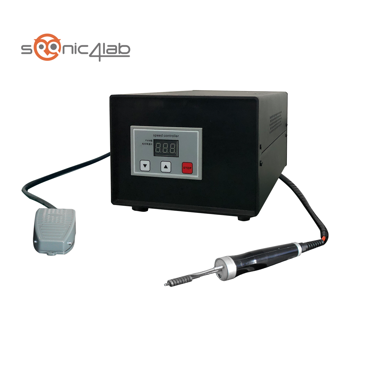
If you want to purchase equipment, please click here.
